X


Comments to #18
All comments (3)
-5

1.
channax 11 year s ago
bbboooooooooooooooooooooorrriiinnnggg ! ! !
2
2.
lullaby 11 year s ago
WOW. This is far for been boring. Pretty cool!
0
3.
jan_kowalski 11 year s ago
yea, cool stuff
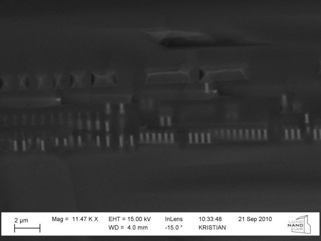
The feature size of the lowest metal layer is around 200-250nm. Since the P-III started out at 250nm process but developed into 180nm (according to wikipedia), the transistor layer must be fairly close to the lowest visible metal layer in the image.