This electronic circuitry is a vital part of the computers we use every day and now you can see just what it looks like on every level.
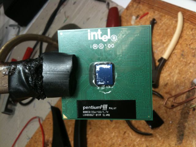
Intel Pentium III™
The blue part in the middle is the actual chip. It needed to be removed in order to further inspect the CPU.
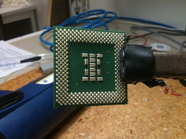
Back side of the circuit board "Up Skirt Shot" containing the CPU. Each pin you see (give or take) should be connected to a pad on the silicon chip. Can also be the most nerve wracking part of building your own PC. Those little pins hate you.
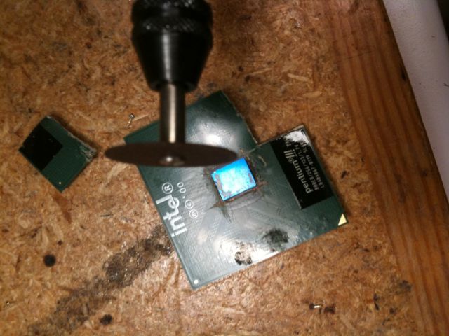
A saw comes in handy sometimes... The Binford 8000 turbo slicer.
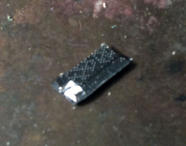
A piece of the processor chip came off. (Thank god for the warranty.)
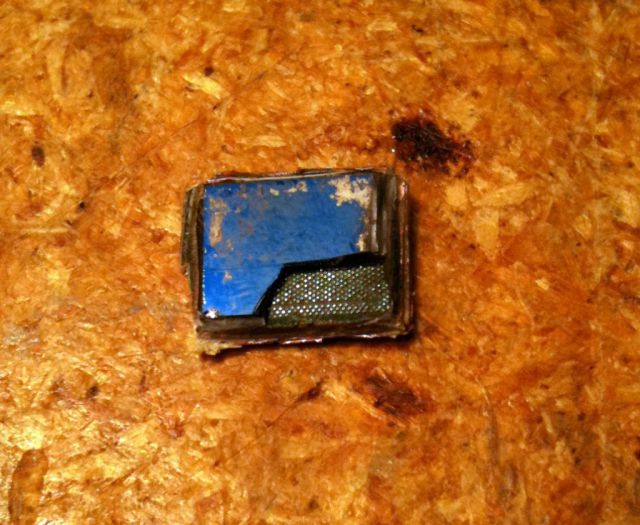
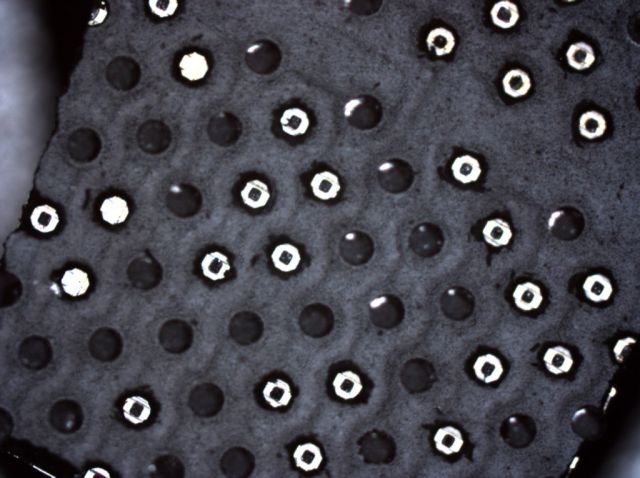
This is the piece that came off. It's been flipped so that the side you see was originally facing towards the circuit board. Each little dot contains a metal pad that connects the interior of the chip to the leads on the board. We are starting to ZOOM in at this point, get ready for the good stuff.
This is a piece of the processor. The side you're seeing was once facing towards the plastic circuit board. Each little hole is a metal pad connecting the interior of the chip to a macroscopic lead on the circuit board.
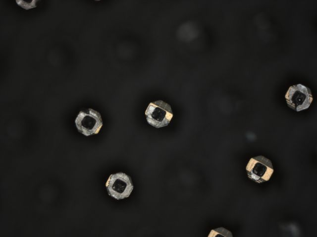
Looking closer, we start seeing some structure inside the holes. (Prepare for a series of tubes)
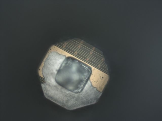
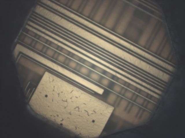
A processor contains many layers of metal leads in order to connect the transistors at the surface of the silicon chip into useful units. The metal layers are clearly visible through the small holes in the chip.
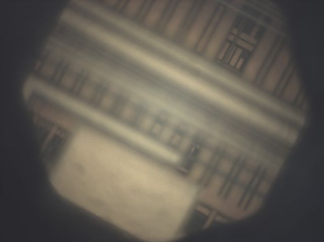
Furthermore, by changing the focus of the microscope, we can see multiple layers within each hole
Focus is on upper layer.
Focus is on middle layer.
Focus is on bottom layer.
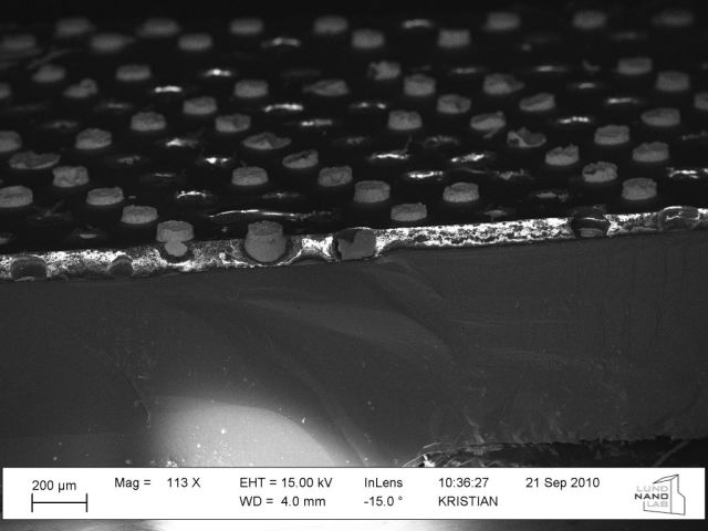
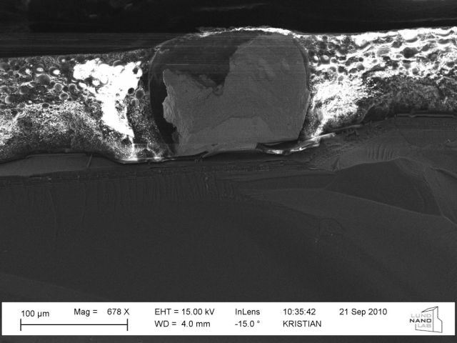
You're looking at the processor chip from the side. In the top part of the image you see the metal pads that were once connected to leads on the circuit board when the chip was bonded face down.
We still don't see a lot. The light stuff between the metal pads is probably some kind of polymer used to fill up the space.
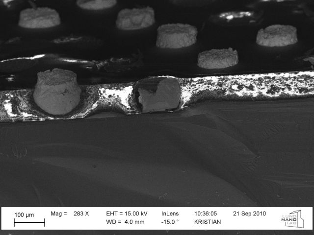
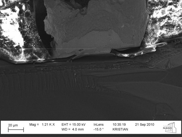
We start to get more detail at the surface of the silicon chip (bottom part of the image. The Si starts somewhere at the bottom of the large metal blob). The texture in the polymer filler (next to the metal blob) could be due to something being mixed into the polymer to increase its thermal conductivity.
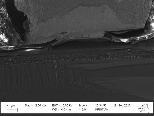
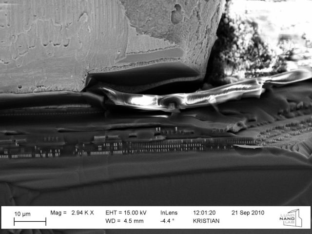
We start seeing something below the metal blob (Yes blob is the scientific term when you are dealing with witchcraft). The vertical lines that are barely visible would be the multiple layers of metal leads. To the right you see the same structure but from another angle since the cut changes direction.
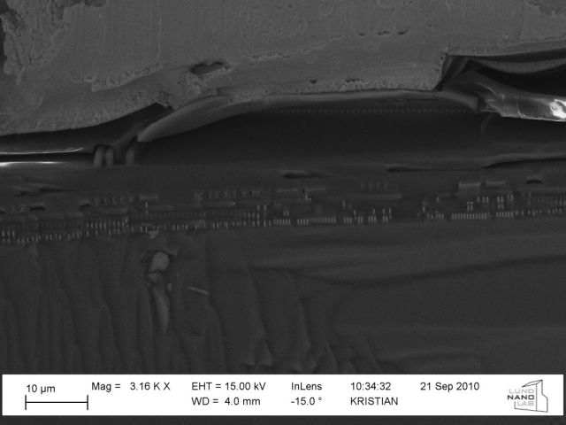
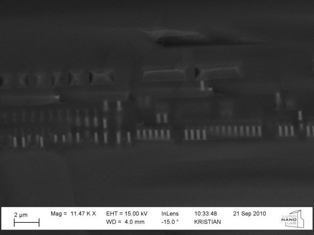
At this point they are clearly visible. I count about six layers of metal leads visible in the image.
The feature size of the lowest metal layer is around 200-250nm. Since the P-III started out at 250nm process but developed into 180nm (according to wikipedia), the transistor layer must be fairly close to the lowest visible metal layer in the image.
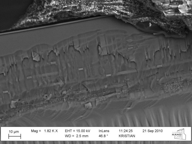
This is not a cross-sectional image but is taken from the top (along the sample normal for those of you who speak science). The processor was accidentally chipped and this is how it looks. Several of the metal layers are visible and as we go down in the image, we go down through the metal layers. It would appear that the bright spots you see are vias connecting leads lying in different layers.

